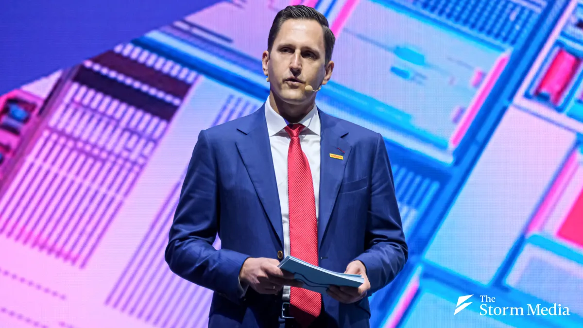
AI chips are being updated faster than ever, and that pace is forcing materials development to speed up right along with them. Benjamin Hein, a member of the executive board of Germany's Merck KGaA, listed on the Frankfurt Stock Exchange as MRK, and chief executive of its electronics business, told the SEMICON Taiwan 2026 Masters Forum on September 2 that semiconductor innovation cycles have compressed from what used to be three or four years down to roughly once a year. Merck, he said, is now using material models to predict a candidate material's key properties before it ever reaches a lab, with confidence levels on some of those predictions reaching around 85 percent.
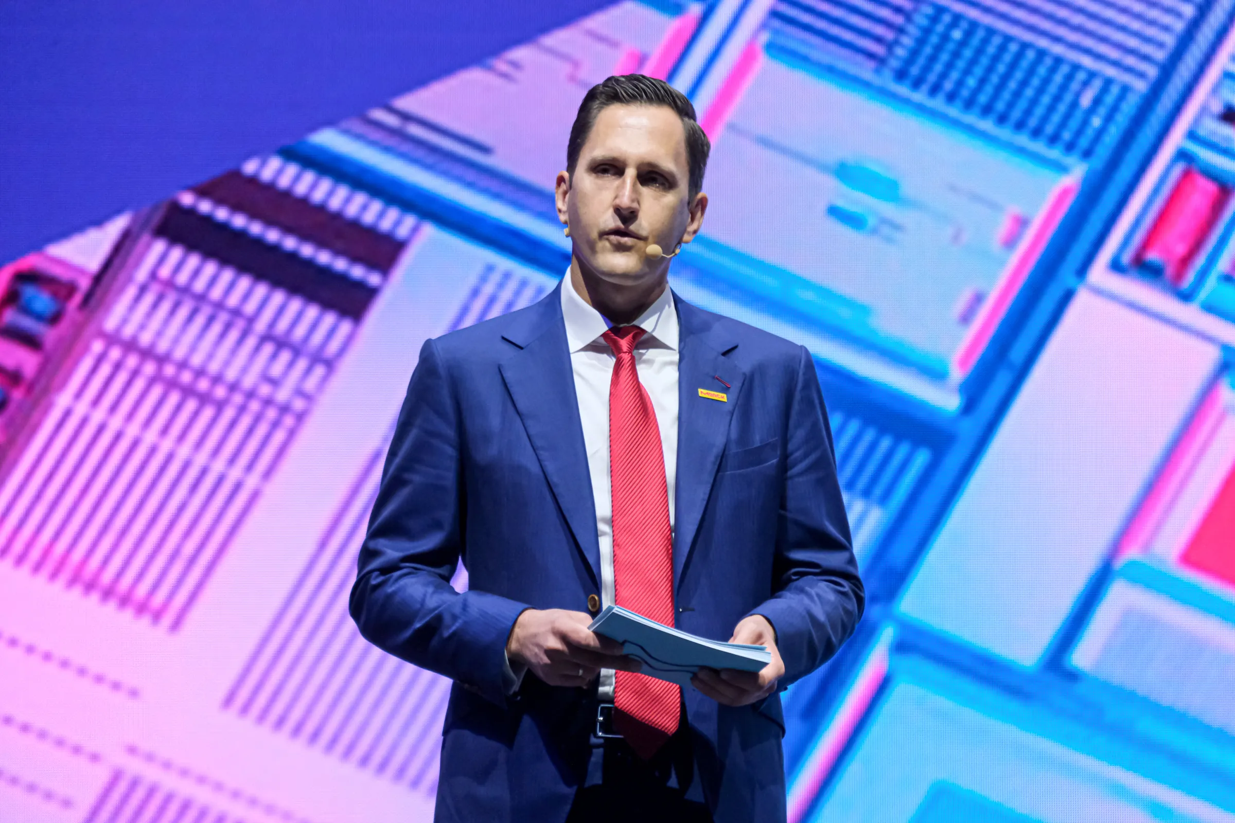
Hein said AI is accelerating its own development, forcing chip architectures, memory and advanced packaging to be refreshed constantly, a pace materials development can no longer match on its old timeline. "We used to have innovation cycles of three or four years. Now that is gradually becoming a cycle of once a year," he said, arguing that keeping pace with AI requires the industry to fold materials, process technology, delivery systems, metrology, defect inspection and software into a single, shared workflow.
AI Performance Costs Are Improving Five To Tenfold Every Year
Hein used what he called "cost to capability," the cost required to reach a given level of model capability or computing output, as his yardstick for AI's pace of progress. By his directional estimate, the cost of AI performance is improving five to tenfold every year, faster than traditional Moore's Law, a trend driven jointly by chips, memory, packaging, networking and software that he described as an accelerated version of Moore's Law.
That improvement, Hein said, does not come from any single component but from the accumulated effect of multiple technologies at once. Faster compute chips, wider high bandwidth memory, shorter interconnect distances from advanced packaging and software that squeezes more out of existing hardware can all combine to push down the cost of reaching a given AI capability. That means semiconductor materials can no longer be optimized for a single specification in isolation. A material can meet every requirement for purity, deposition speed or electrical properties and still fail to deliver the stability and yield mass production demands if it is not also compatible with the delivery equipment, process conditions and measurement methods around it.
Screening Materials With Models Before They Ever Reach A Lab
To keep up with shorter product cycles, Merck has already built AI into its materials research. Hein said the company uses its SYNTHIA software along with material models to predict a candidate's key properties before it is ever actually synthesized, with confidence levels on some predictions reaching around 85 percent. The model helps researchers narrow down a large pool of candidate molecules or formulations to the ones most likely to meet requirements before they ever move to lab verification, cutting down on wasted experiments and shortening development time. "Materials AI is not a future concept. It already exists today," Hein said. He cautioned, however, that the roughly 85 percent figure reflects the model's confidence in predicting certain material properties, not the accuracy of every materials experiment or the odds of eventual mass production success. Materials still have to go through physical synthesis, process testing, customer validation and reliability evaluation before they can formally enter production.
A Molybdenum Precursor Delivery System Pushes Utilization Past 99 Percent
Hein pointed to molybdenum thin film materials as an example of how an integrated workflow can raise material efficiency. Merck has integrated its MoO2Cl2 molybdenum precursor with a solid state material delivery system, controlling storage, heating and delivery conditions to push material utilization above 99 percent. A chemical molecule by itself, he said, is only part of the solution. If a material cannot be delivered reliably to the process chamber or kept consistent across different production batches, lab results that look good on paper may not translate into results in a mass production environment.
Advanced Packaging Is Starting To Look Like Front End Fabrication
AI chips are also blurring the line between front end and back end manufacturing processes. Hein said advanced packaging's requirements around purity, defects and process control are beginning to approach front end wafer fabrication standards, a shift he described as the back end taking on front end characteristics. Deposition, patterning, planarization, cleaning and metrology techniques once used mainly in front end wafer processing are now showing up in 2.5D and 3D packaging and in wafer to wafer and die to wafer stacking. As dies get thinner and bonding gaps shrink, tiny particles, surface irregularities or material residue can all cause a connection to fail. Merck's Unity-SC unit has developed a phase shift diffraction technique that combines metrology and defect inspection for use on wafer and die stacking structures, reading bonding interfaces and structural changes.
Hein said advanced packaging, co-packaged optics, quantum computing and neuromorphic computing will not replace one another but will instead develop in parallel. Facing an innovation pace that now resets every year, he said, AI models can help narrow the field of candidate materials, but the real key to shortening time to market remains connecting materials, process technology, equipment, metrology and mass production validation into a single working pipeline.
(Related:
Chunghwa Precision Test Debuts AI Agent That Cuts Engineering Simulations From Hours To Seconds
|
Latest
)